

Industries · 8 min read
Semiconductor wafer inspection with a bright-field camera at intake
A cracked wafer rejected at intake costs a wafer. Found after lithography it costs every step spent on it. Three classes, and masks where extent decides.
Summary
This post puts a bright-field camera at wafer intake and works through cracks, scratches and edge chips as classes, the specular highlight that looks like a scratch, tiling the frame so a thin defect survives the model's input size, and masks where extent decides rework against reject. It concludes that a tightened defect spec is the day the old labels go wrong without a pixel changing. It is for fab process and quality engineers.
Finn Ellingwood · Engineer · Sep 25, 2026
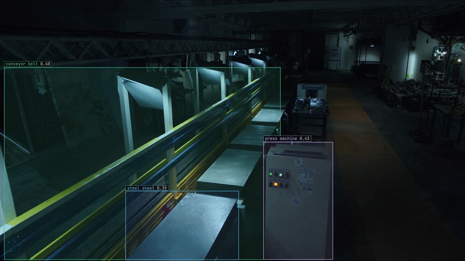
Steel sheet passing an inspection station on a stamping line, generated scene with detections from our model
The wafers arrive at intake in a cassette of twenty-five, and the technician on the 6 am shift holds each one up to the light on the way into the first tool. A wafer with a crack in it that goes into lithography will be found at the end of the line, after every step has been spent on it. The look takes a few seconds per wafer and catches the cracks that are big enough to see by eye at arm's length. The ones that are not are the expensive ones.
A bright-field camera at intake looks at every wafer the same way, at a resolution the eye does not have, before the line spends anything on it.
Cracks, scratches and edge chips each get a bounding box and a response
The classes come from what the fab does about each. A crack is a reject, whatever its size, because a cracked wafer breaks in a later tool. A scratch is a severity call: light ones are cleaned or reworked, deep ones across an active area are rejected. An edge chip is a reject if it is over a written size and a monitored wafer if under. Three classes, three different downstream actions, and the model's job is to tell them apart on a mirror-finish surface where all three are a few pixels wide.
The frames come from the intake camera at its fixed mount, under the bright-field ring light, with the wafer in the chuck where the handler leaves it. You type the three classes once, Lexi proposes a bounding box on every defect in every frame, and a person checks the proposals before anything trains. The person is there for one thing above all.
The specular highlight is the labeler's hardest call
A wafer is a mirror. Under a bright-field light the surface throws back the ring light as a highlight, and a highlight at the wrong angle is a bright streak that looks exactly like a scratch. A labeler who boxes the highlight teaches the model that light is a defect, and the model then rejects a clean wafer every time the chuck sits a degree off.
The rule, written before labeling starts, is that a streak is a scratch only if it is still there when the wafer is tilted. At labeling time that means the labeler has two frames of the same wafer at two chuck positions and boxes only what appears in both. That doubles the frames and halves the arguments. Labels on an inspection set like this come back at up to 99.9% accuracy when every one is checked, and the checking here is almost entirely the highlight question.
The other labeling rule is about thin defects. A scratch across a wafer is long and one pixel wide, and a loose box around it is mostly clean silicon. The box hugs the scratch, and a scratch that curves is two boxes rather than one large one. Consistency matters more than the choice: a set where half the scratches are loose and half are tight is a set the model cannot learn from.
A thin defect needs the frame tiled before the model sees it
The intake camera at station 1 produces a large frame and the model takes a smaller input. Scaling the whole wafer down to fit loses the one-pixel scratch entirely, and a model evaluated on scaled frames reports a recall on scratches that has nothing to do with what it will find at intake.
The answer is to tile: cut the frame into overlapping patches at full resolution, run the model on each, and merge the boxes across the seams. A defect on the seam between two tiles is found in both and merged into one box; the overlap is set wider than the largest defect so nothing falls between. Tiling costs inference time per wafer, which at intake is available, since a wafer waits in the cassette anyway.
The surface defect detection use case says the same of any reflective part: the defect is small and low-contrast, a lighting artefact looks exactly like a flaw, and the good parts outnumber the bad by so much that the training set is unbalanced by construction. Frames with defects are kept at a far higher share than they occur, and clean wafers are kept too, so the model learns what the chuck edge and the notch look like when nothing is wrong.
A mask where the extent decides rework or reject
For cracks a box is enough, because any crack is a reject and the box says there is one. For scratches and chips the decision is on size, and a box does not carry the size. A mask over the scratch gives its length; a mask over the chip gives its area against the written limit. So the pipeline boxes every defect, and for the two classes decided on extent it adds a mask, labeled only on those classes to keep the labeling cost where the decision is.
The outcome is a rule written as a sentence, with a severity and a cooldown, approved before it goes live: a crack or an over-limit chip on a wafer at intake, high, to the intake tool's screen and the process engineer in Slack. The frame arrives with the defect drawn on it and the measurement beside it, so the engineer sees the chip and its area rather than a wafer ID and a verdict.
In our manufacturing work the inspection models hold 99%+ accuracy maintained in production, and a wafer intake is where that figure is worth the most per frame, since every wafer that passes intake has the whole line ahead of it.
The unsure wafer goes to a person before it goes to lithography
Some wafers are plainly clean and some plainly cracked. Between them is a band: a streak the model boxed at low confidence, a chip near the limit, a mark that could be a highlight. Those wafers are held at intake and the frame goes to the technician with the box drawn on it, which is the same look the technician gave every wafer before, now given only to the wafers that need it.
LexData takes the intake model through its whole life. You type what to look for, Lexi puts a bounding box on every frame, and a person checks each label before anything trains on it. The model then watches the intake camera, in the cloud, on your servers, or on a runner beside the recorder. Frames it is unsure of come back to a person, the corrections retrain it, and the new version replaces the old one with no downtime. On a wafer line the doubted frames are the highlights and the near-limit chips, and the technician's verdicts on those are what the next version learns.
One aside. The technician on the 6 am shift still holds up one wafer per cassette to the light, and it is the one the model was surest about, on the grounds that a wafer nobody doubted is the one nobody looked at.
A tightened defect spec makes the old labels wrong without changing a pixel
The customer's spec for the next product tightens the chip limit in March. A chip that was monitored last month is a reject this month. The wafers look the same, the camera is the same, and every label that said "monitor" on a chip of that size is now wrong. The drift catalog calls this a spec change: the pixels are identical and every label you own has moved.
Because the model finds and measures and the rule decides, the fix is the number in the rule, changed on the day the spec arrives. A model that had been trained to output reject or monitor directly would have to be relabeled and retrained, and would go on passing chips in the meantime. The signal, if the spec change goes unrecorded somewhere, is the correction rate: the technician starts overriding the intake verdict on wafers it passed, and the override rate climbs until somebody asks what changed.
My own view is that the limit in the rule should be read from the same spec document the fab already controls, however awkward it is to wire. A limit copied by hand into a rule is the limit that will be wrong the week the spec moves. How the labels get checked before training is in the labeling doc.
See it on your own footage.
Start with your footageMore in Industries
Industries · 7 min read
Counting the screws in a kit with object detection over the bench
A camera over the kitting bench counts every screw and bottle one box at a time. Exact for kits, a band for cases, and a half-hidden item is a written rule.
Rajiya Sultana · Sep 25, 2026
Industries · 7 min read
Automated water meter reading with a camera in the vault
Ten digit classes in a fixed row turn a truck roll into a frame. A rolling digit and condensation on the glass are the frames that come back to a person.
Stephen Biswas · Sep 25, 2026
Industries · 7 min read
Body-in-white inspection with a station camera on unpainted steel
Dents on a bare body shell hide in the reflections. Masks give the extent, a second pass decides reportable, and a tightened tolerance is a spec change.
Finn Ellingwood · Sep 25, 2026